-
Products
- Gas analysis systems
- GAOS SENSON gas analyzers
- GAOS MS process mass spectrometry
- MaOS HiSpec ion mobility spectrometer
- MaOS AxiSpec ion mobility spectrometer
- Applications
- News
- Events
- About us
|
o Control of surface defect depth o Measurement of surface roughness after mechanical, ionic treatment
o Caliber measurement (in microrange and nanorange) o Measurement of surface nanohoughness o Measurement of structures with a height of one interatomic spacing of a silicon crystal lattice |
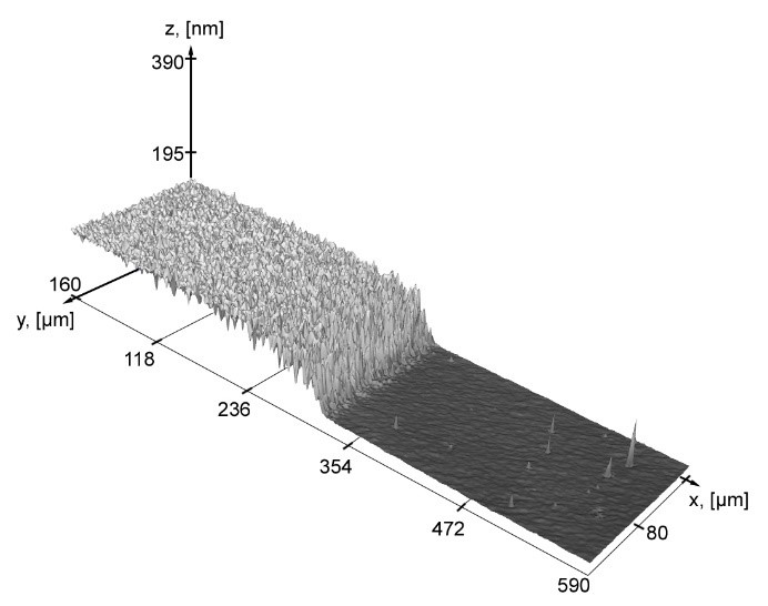
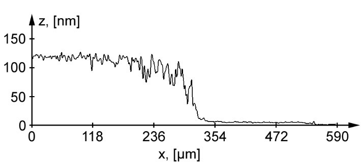
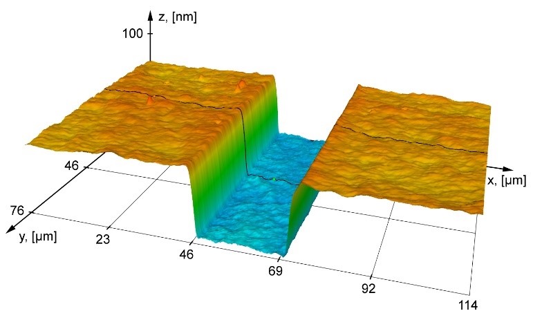
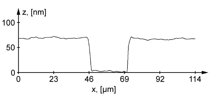
o Investigation of thin film deposition process - thin film thickness measurement on the witness sample o Investigation of the surface treatment process in the nanoscale range - measurement of surface nano roughness before and after processing
|
|
 |
|
Palladium film on the silicon substrate, average thickness ~ 120 nm |
|
 |
 |
|
Chromium film on the glass substrate, average thickness ~ 66 nm |
|
|
 |
|
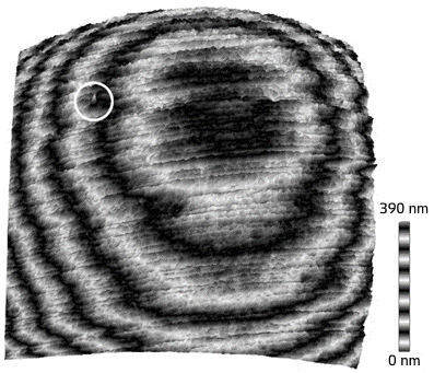
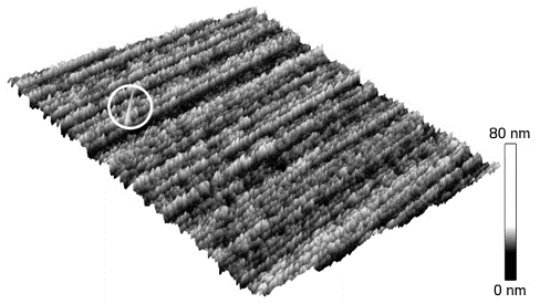
Prosthesis of hip joint head: a – measured surface (color bar’s period is 60 nm), b – filtered result of a (measured roughness Sa = 3,7 nm) |
|
|
 |
|
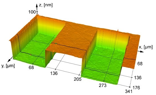
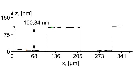
Caliber, the metric of roughness Rz, industrial standard 1st category, nominal value 101 nm ± 3% |
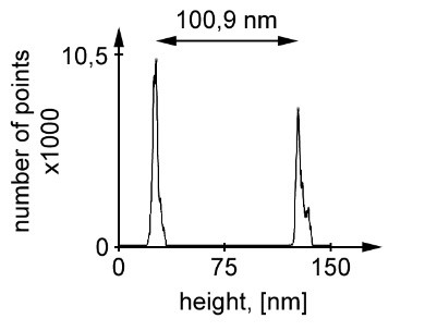 |
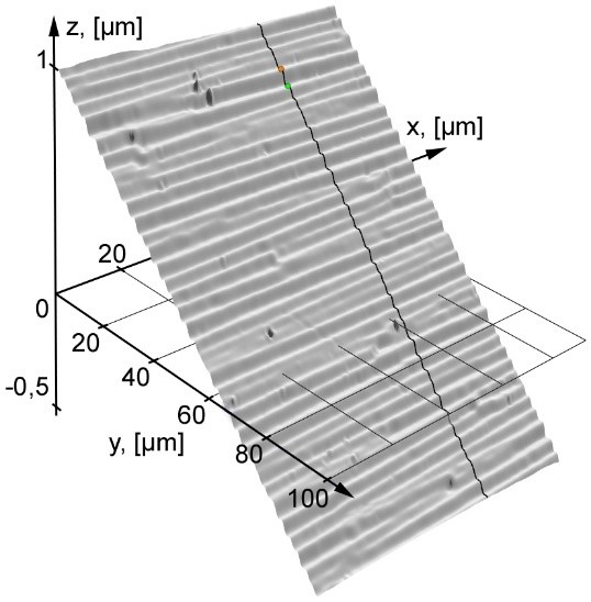 |
 |
|
Echelon of atomic steps |
|
|
|
Terraces on the surface of Si crystal, height 0,314 nm |
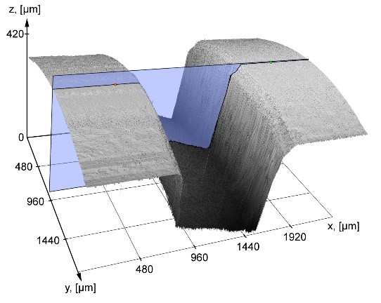
|
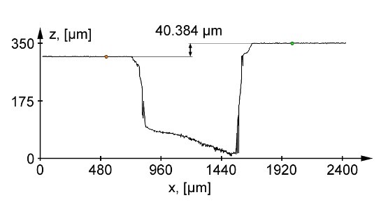 |
|
|
Certified height caliber 40 ± 1,2 µm |
 |
 |
|
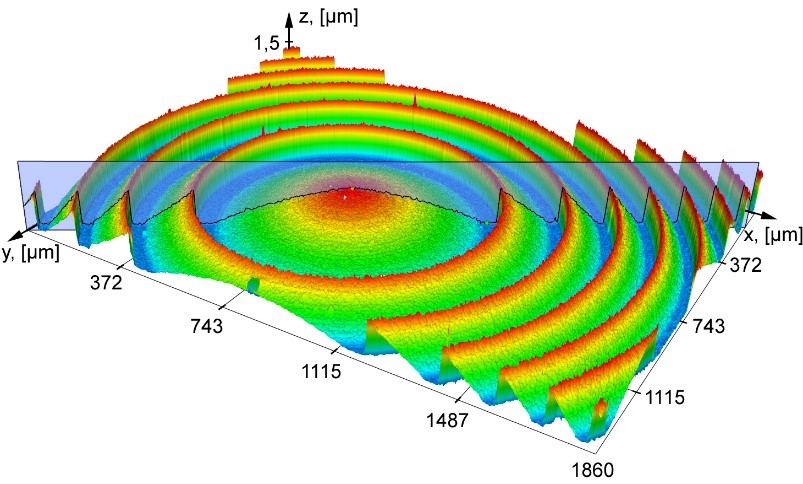
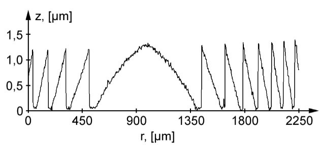
Diffraction element – Fresnel lens |
|
|
|
Diffraction element, height 3,7 µm |
|
|
 |
|
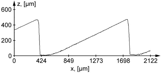
Diffraction element, height 3,7 µm |
|
 |
 |
|
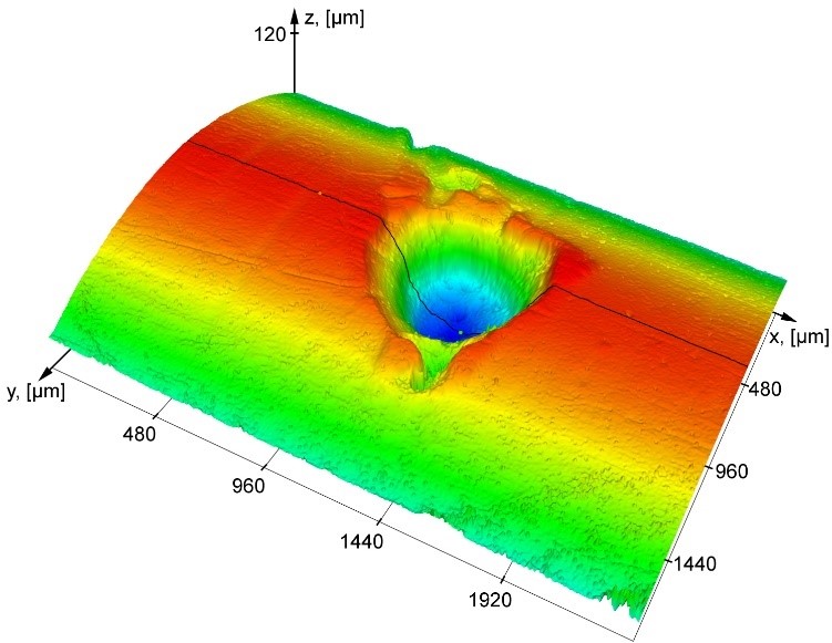
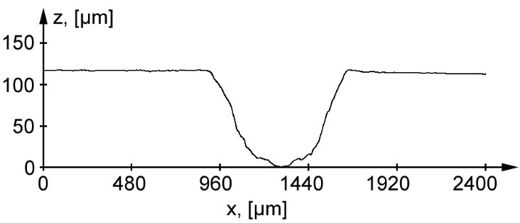
Defect of a cylindrical surface |
 |
 |
|
a |
b |
|
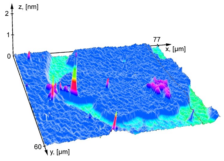
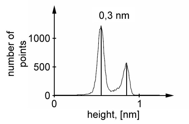
Fragment of surface nano relief that contains monoatomic layers of Si (111): a – 3D reconstructed surface, b – height distribution of selected surface area |
|
 |
 |
 |
|
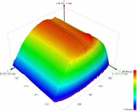
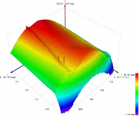
Surface of bullet |
||
 |
 |
 |
|
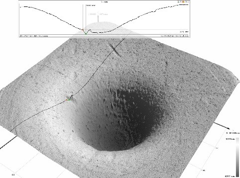
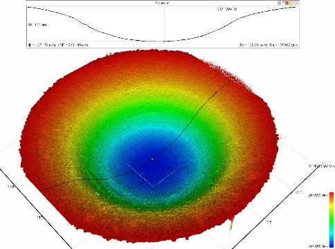
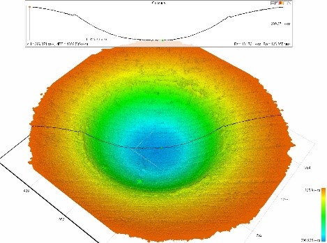
Surface of detonator |
||